| CPC H10B 12/485 (2023.02) [G11C 5/063 (2013.01); H01L 21/02532 (2013.01); H01L 21/02595 (2013.01); H01L 21/02598 (2013.01); H10B 12/482 (2023.02); H01L 21/02609 (2013.01)] | 16 Claims |
|
1. A method for forming a storage node contact structure, comprising steps of:
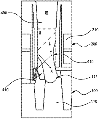
providing a substrate having a surface on which bit line structures are formed, a contact hole being formed between the bit line structures;
forming a groove at a part, corresponding to an active region, of a bottom of the contact hole, an included angle between an axial direction of an opening of the groove and a vertical direction being greater than 0 degree and less than 90 degrees; and
growing a silicon crystal from the groove in the contact hole by using an epitaxial growth process, and controlling growth rates of the silicon crystal in a first direction and a second direction in a growth process, to enable the growth rate of the silicon crystal in the first direction to be greater than the growth rate of the silicon crystal in the second direction at a beginning of growth, and to enable the growth rate of the silicon crystal in the first direction to be equal to the growth rate of the silicon crystal in the second direction at an end of the growth, thereby separately forming gaps between the silicon crystal and side walls of both the bit line structures in the second direction,
wherein the first direction is the axial direction of the opening of the groove, and the second direction is perpendicular to the first direction in a vertical plane.
|