| CPC H10B 12/485 (2023.02) [H10B 12/31 (2023.02); H10B 12/34 (2023.02); H10B 12/488 (2023.02)] | 13 Claims |
|
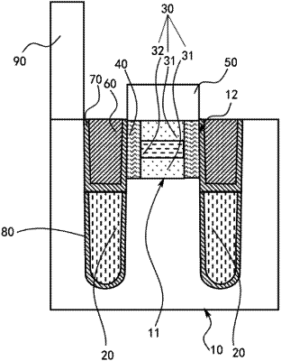
1. A semiconductor structure, comprising:
a substrate;
word lines, located in the substrate, wherein a bit line contact hole is provided between each two adjacent word lines;
bit line contact plugs, located in the bit line contact holes; and
first isolation layers, located on side walls of the bit line contact holes and covering side walls of the bit line contact plugs,
wherein a bit line contact plug among the bit line contact plugs is a three-layer structure comprising a metal material and two layers of polycrystalline silicon, and
wherein the metal material is sandwiched between the two layers of polycrystalline silicon.
|