| CPC H10B 12/482 (2023.02) [G11C 5/063 (2013.01)] | 15 Claims |
|
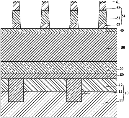
1. A method for manufacturing a semiconductor structure, comprising:
providing a base;
sequentially stacking an initial conductive layer, an initial first dielectric layer, an initial first mask layer, an initial second dielectric layer, an initial second mask layer and a photoresist layer with a pattern on the base;
etching part of the initial second mask layer and part of the initial second dielectric layer by taking the photoresist layer as a mask, so as to form a second dielectric layer with a trapezoidal structure, a width of the trapezoidal structure being gradually increased from an end departing from the base to an end close to the base; and
etching part of the initial first mask layer, part of the initial first dielectric layer, part of the initial conductive layer and part of the base by taking the second dielectric layer as a mask, so as to form bit line structures.
|