| CPC H10B 12/053 (2023.02) [H10B 12/34 (2023.02)] | 16 Claims |
|
1. A method for forming a semiconductor structure, comprising:
providing a semiconductor substrate, the semiconductor substrate having a plurality of separate active areas that are isolated from each other by shallow trench isolation areas;
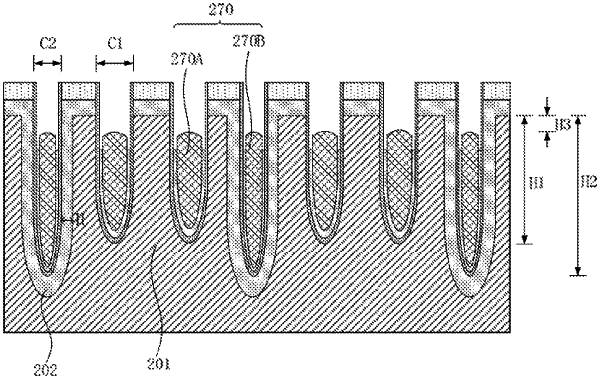
forming trenches by etching the active areas and the shallow trench isolation areas, wherein the trenches comprise first trenches and second trenches, the first trenches are located in the active areas, the second trenches are located in the shallow trench isolation areas, and the first trenches have a width greater than a width of the second trenches; and
forming word lines in the trenches, wherein the word lines comprise first word lines and second word lines, each of the first word lines is located in a respective first trench of the first trenches, each of the second word lines is located in a respective second trench of the second trenches, and the first word lines have a width greater than a width of the second word lines,
wherein in the step of forming the trenches by etching the active areas and the shallow trench isolation areas, an etch rate of an etching substance on the shallow trench isolation areas is less than an etch rate of the etching substance on the active areas, so that the first trenches have the width greater than the width of the second trenches,
wherein the shallow trench isolation areas are silicon dioxide isolation areas, the active areas are silicon active areas, and forming the trenches by etching the active areas and the shallow trench isolation areas comprises:
forming a mask layer and a photoresist layer on the semiconductor substrate;
forming a window by patterning the photoresist layer;
exposing the silicon active areas and the silicon dioxide isolation areas by etching the mask layer along the window;
using Cl2, HBr, CF4, and CHF3 as gas sources, and etching, for a first time, the silicon active areas and the silicon dioxide isolation areas using a plasma process for a period of time; and
using the CF4 and the CHF3 as gas sources, and etching, for a second time, the silicon active areas and the silicon dioxide isolation areas using the plasma process for a second period of time to form the first trenches and the second trenches.
|