| CPC H10B 12/05 (2023.02) [G11C 11/4085 (2013.01); H01L 29/66666 (2013.01); H01L 29/7827 (2013.01); H10B 12/315 (2023.02); H10B 12/488 (2023.02)] | 8 Claims |
|
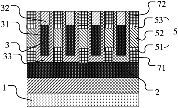
1. A manufacturing method of a semiconductor structure, comprising:
forming a to-be-etched body, the to-be-etched body comprising a base substrate, an insulator located on one side of the base substrate and a plurality of bit lines, the bit lines being located in the insulator, and the plurality of bit lines being distributed at intervals along a first direction and extending along a second direction;
forming a plurality of second grooves, which are distributed at intervals along the second direction and extend along the first direction, on one side of the insulator facing away from the bit lines;
sequentially forming a word line and a fourth insulating layer in each second groove, the fourth insulating layer being located on one side of the word line facing away from a bottom of the second groove;
forming a plurality of through holes distributed in an array on one side of the insulator facing away from the base substrate, orthographic projection of each through hole on the base substrate at least partially coinciding with an orthographic projection of a respective bit line on the base substrate, the through hole extending to a surface of the bit line, and in the second direction, an orthographic projection of only one word line on the base substrate being located between the orthographic projections of two adjacent through holes on the base substrate;
forming a fifth insulating layer on one side of the word line exposed to the through hole; and
forming a first source or drain part, an active part and a second source or drain part in each through hole, the first source or drain part being located on one side of a respective bit line, the active part being located on one side of the first source or drain part facing away from the bit line, and the second source or drain part being located on one side of the active part facing away from the bit line.
|