| CPC H10B 10/18 (2023.02) [H01L 21/0259 (2013.01); H01L 21/823807 (2013.01); H01L 21/823814 (2013.01); H01L 21/823821 (2013.01); H01L 21/823871 (2013.01); H01L 27/092 (2013.01); H01L 29/0665 (2013.01); H01L 29/0847 (2013.01); H01L 29/41733 (2013.01); H01L 29/41791 (2013.01); H01L 29/42392 (2013.01); H01L 29/66545 (2013.01); H01L 29/66742 (2013.01); H01L 29/66795 (2013.01); H01L 29/7851 (2013.01); H01L 29/78618 (2013.01); H01L 29/78696 (2013.01); H10B 12/50 (2023.02)] | 20 Claims |
|
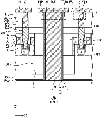
1. A semiconductor device, comprising:
a substrate including a logic cell region and a connection region;
a dummy transistor on the connection region;
an intermediate connection layer on the dummy transistor, the intermediate connection layer including a connection pattern electrically connected to the dummy transistor;
a first metal layer on the intermediate connection layer;
an etch stop layer between the intermediate connection layer and the first metal layer, the etch stop layer covering a top surface of the connection pattern; and
a penetration contact extended from the first metal layer toward a bottom surface of the substrate penetrating the connection region,
wherein an upper portion of the penetration contact protrudes above the etch stop layer,
the first metal layer including a first interconnection line, a second interconnection line, and a via below the second interconnection line,
the via penetrates the etch stop layer and connects the second interconnection line to the connection pattern, and
a top surface of the penetration contact is in direct contact with a bottom surface of the first interconnection line.
|