| CPC H05K 3/467 (2013.01) [H05K 1/0298 (2013.01); H05K 1/0313 (2013.01); H05K 3/0023 (2013.01); H05K 3/188 (2013.01); H05K 2203/06 (2013.01); H05K 2203/0723 (2013.01)] | 7 Claims |
|
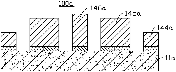
1. A circuit board comprising:
a substrate comprising a base layer, a first metal layer formed on the base layer, and a seed layer formed on the base layer;
a first circuit layer located on the substrate and comprising the first metal layer and a signal layer formed on a surface of the first metal layer;
a second circuit layer coupled to the first circuit layer and comprising the first metal layer, the seed layer, and a connection pillar formed on a surface of the first metal layer and the seed layer; and
a third circuit layer coupled to the second circuit layer and comprising the seed layer and a coil formed on a surface of the seed layer, wherein a sheet resistance of the first metal layer is larger than a sheet resistance of the seed layer.
|