|
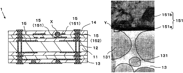
1. A wiring board comprising: at least an insulating layer containing particles of silica, and a wiring conductor layer located on the insulating layer, wherein among the particles of the silica contained in the insulating layer, some particles of the silica are partially exposed on a surface of the insulating layer, the wiring conductor layer comprises a seed layer located on the insulating layer and containing a metal, and a plated conductor layer located on the seed layer, and a non-crystalline layer of the silica and a non-crystalline layer of the metal of the seed layer are present at contact portions between exposed portions of the particles of the silica and the seed layer; wherein a thickness of the non-crystalline layer of the metal is larger than a thickness of the non-crystalline layer of the silica.
|
