| CPC H05K 1/0274 (2013.01) [H01Q 1/48 (2013.01); H05K 1/0243 (2013.01); H05K 1/16 (2013.01); H01Q 23/00 (2013.01); H05B 45/30 (2020.01); H05K 2201/10098 (2013.01); H05K 2201/10106 (2013.01)] | 11 Claims |
|
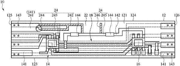
1. A circuit board, comprising:
a substrate, comprising a first circuit layer and a second circuit layer opposite to each other;
a driver circuit, located on the first circuit layer;
at least one light-emitting element, located on the first circuit layer and electrically connected to the driver circuit, so that the driver circuit controls the light-emitting element to emit light;
a grounding circuit, located on the second circuit layer and electrically connected to the driver circuit, wherein the grounding circuit comprises a plurality of conductive traces, and the conductive traces are arranged toward one side in central to form a clearance area on the second circuit layer; and
an antenna unit, located on the first circuit layer and corresponding to the clearance area to receive and transmit a radio frequency signal.
|