| CPC H05K 1/0251 (2013.01) [H05K 3/10 (2013.01); H05K 2201/09236 (2013.01)] | 19 Claims |
|
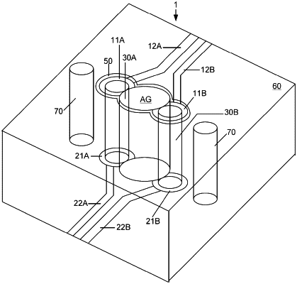
1. A conductive pattern configured to be applied over a substrate, comprising:
a dielectric region; and
a pair of complementary conductive traces, each comprising a linear portion and a terminal portion,
wherein the linear portions of the pair of traces extend linearly abreast each other at a first separation,
wherein the terminal portions of the pair of traces are arranged adjacent to each other, and the terminal portions of the pair of complementary conductive traces are arranged in the dielectric region,
wherein the terminal portions of the pair of traces comprises a pair of circular arc profiles with a pair of complementary notches facing toward each other,
wherein a gap between the complementary notches of the terminal portions is wider than the first separation,
wherein the pair of complementary conductive traces and the dielectric region are exposed from a solder mask layer disposed over the substrate.
|