| CPC H05B 45/10 (2020.01) [H05B 45/325 (2020.01); H05B 45/37 (2020.01)] | 1 Claim |
|
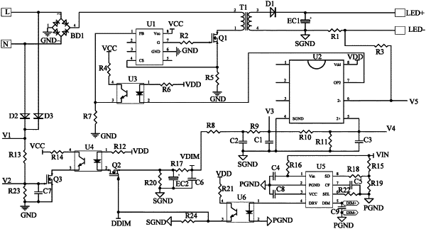
1. A six-in-one dimming circuit, comprising a main control power circuit, a silicon controlled rectifier signal acquisition circuit, a DIM signal conversion circuit, a silicon controlled rectifier signal conversion circuit, and an output current control circuit, wherein the main control power circuit comprises a live wire and a neutral wire that are connected to a silicon controlled rectifier dimmer or an electronic low-voltage (ELV) dimmer or a magnetic low-voltage (MLV) dimmer, and further comprises a power output positive electrode and a power output negative electrode that are connected to a 0-10 V dimmer or a resistance dimmer or a pulse width modulation (PWM) dimmer; the DIM signal conversion circuit comprises a DIM signal positive input terminal and a DIM signal negative input terminal; a signal acquisition terminal of the silicon controlled rectifier signal acquisition circuit is connected to the live wire and the neutral wire of the main control power circuit; the silicon controlled rectifier signal conversion circuit comprises an input terminal separately connected to an output terminal of the silicon controlled rectifier signal acquisition circuit and an output terminal of the DIM signal conversion circuit, and further comprises an output terminal connected to an input terminal of the output current control circuit; and the output current control circuit comprises an output terminal connected to a feedback signal input terminal of the main control power circuit, and further comprises a voltage signal acquisition terminal connected to the power output negative electrode of the main control power circuit;
the main control power circuit comprises the live wire, the neutral wire, a rectifier bridge, a transformer, a main control chip, a first metal-oxide-semiconductor field effect transistor (MOSFET), a first diode, a first electrolytic capacitor, a first resistor, a second resistor, and a fifth resistor; the rectifier bridge comprises a pin 2 connected to the live wire, a pin 3 connected to the neutral wire, and a pin 4 connected to a pin 2 of the transformer; the transformer comprises a pin 1 connected to a drain of the first MOSFET and a pin 3 connected to an anode of the first diode; a pin 4 of the transformer, a negative electrode of the first electrolytic capacitor, and a first terminal of the first resistor are connected to a signal ground; a cathode of the first diode is connected to a positive electrode of the first electrolytic capacitor and the power output positive electrode, respectively; a second terminal of the first resistor is connected to the power output negative electrode; the second resistor is connected in series between a pin 7 of the main control chip and a gate of the first MOSFET; a pin 4 of the main control chip is connected to a source of the first MOSFET and a first terminal of the fifth resistor, respectively; and a pin 1 of the rectifier bridge, a pin 6 of the main control chip, and a second terminal of the fifth resistor are connected to a power supply ground (GND);
the silicon controlled rectifier signal acquisition circuit comprises a second diode, a third diode, a third MOSFET, a fourth optical coupler, a seventh capacitor, a twelfth resistor, a thirteenth resistor, a fourteenth resistor, and a twenty-third resistor; an anode of the second diode is connected to the neutral wire, and an anode of the third diode is connected to the live wire; a cathode of the second diode is connected to a cathode of the third diode and a first terminal of the thirteenth resistor, respectively; a second terminal of the thirteenth resistor, a first terminal of the twenty-third resistor, a first terminal of the seventh capacitor, and a gate of the third MOSFET are connected; a second terminal of the twenty-third resistor, a second terminal of the seventh capacitor, and a source of the third MOSFET are connected to the power supply ground; the fourth optical coupler comprises a pin 1 connected to a first terminal of the twelfth resistor, a pin 3 connected to a drain of the third MOSFET, and a pin 4 connected to a first terminal of the fourteenth resistor; and a second terminal of the fourteenth resistor is connected to a pin 8 of the main control chip;
the DIM signal conversion circuit comprises a digital signal conversion chip, a sixth optical coupler, a fourth capacitor, a fifth capacitor, an eighth capacitor, a ninth capacitor, a fifteenth resistor, a sixteenth resistor, an eighteenth resistor, a nineteenth resistor, a twenty-first resistor, a twenty-second resistor, and a twenty-fourth resistor; the digital signal conversion chip comprises a pin 1 respectively connected to a first terminal of the sixteenth resistor and a first terminal of the fourth capacitor, a pin 3 connected to a first terminal of the eighth capacitor, and a pin 4 connected to a pin 1 of the sixth optical coupler; a pin 5 of the digital signal conversion chip and a first terminal of the ninth capacitor are connected to the DIM signal positive input terminal; a second terminal of the ninth capacitor is connected to the DIM signal negative input terminal; the digital signal conversion chip further comprises a pin 6 connected to a first terminal of the twenty-second resistor, a pin 7 connected to a first terminal of the fifth capacitor, and a pin 8 connected to a first terminal of the eighteenth resistor; a second terminal of the sixteenth resistor is connected to a first terminal of the fifteenth resistor; a second terminal of the fifteenth resistor is connected to a second terminal of the eighteenth resistor and a first terminal of the nineteenth resistor, respectively; a pin 3 of the sixth optical coupler is connected to a first terminal of the twenty-fourth resistor; a second terminal of the twenty-fourth resistor is connected to the signal ground; a pin 4 of the sixth optical coupler is connected to a first terminal of the twenty-first resistor; and a pin 2 of the digital signal conversion chip, a second terminal of the fourth capacitor, a second terminal of the eighth capacitor, a pin 2 of the sixth optical coupler, a second terminal of the ninth capacitor, a second terminal of the twenty-second resistor, a second terminal of the fifth capacitor, and a second terminal of the nineteenth resistor are connected to a power ground (PGND);
the silicon controlled rectifier signal conversion circuit comprises a second MOSFET, a seventeenth resistor, a twentieth resistor, a second electrolytic capacitor, and a sixth capacitor; the second MOSFET comprises a drain connected to a pin 2 of the fourth optical coupler and a gate connected to the pin 3 of the sixth optical coupler; a source of the second MOSFET is connected to a first terminal of the seventeenth resistor, a first terminal of the twentieth resistor, and an anode of the second electrolytic capacitor, respectively; a second terminal of the seventeenth resistor is connected to a first terminal of the sixth capacitor; and a second terminal of the twentieth resistor, a cathode of the second electrolytic capacitor, and a second terminal of the sixth capacitor are connected to the signal ground; and
the output current control circuit comprises a dual operational amplifier, a third optical coupler, a third resistor, a fourth resistor, a sixth resistor, a seventh resistor, an eighth resistor, a ninth resistor, a tenth resistor, an eleventh resistor, a first capacitor, a second capacitor, and a third capacitor; the eighth resistor comprises a first terminal connected to the second terminal of the seventeenth resistor and a second terminal connected to a first terminal of the ninth resistor and a first terminal of the second capacitor, respectively; a second terminal of the ninth resistor is connected to a first terminal of the first capacitor and a first terminal of the tenth resistor, respectively; a second terminal of the tenth resistor is connected to a first terminal of the eleventh resistor, a first terminal of the third capacitor, and a pin 5 of the dual operational amplifier, respectively; a first terminal of the third resistor is connected to a second terminal of the first resistor; the dual operational amplifier comprises a pin 6 connected to a second terminal of the third resistor and a pin 7 connected to a pin 2 of the third optical coupler; the third optical coupler comprises a pin 1 connected to a first terminal of the sixth resistor, a pin 3 respectively connected to a first terminal of the seventh resistor and a pin 1 of the main control chip, and a pin 4 connected to a first terminal of the fourth resistor; a second terminal of the fourth resistor is connected to a pin 8 of the main control chip; a second terminal of the seventh resistor is connected to the power supply ground; a pin 8 of the dual operational amplifier is respectively connected to a second terminal of the sixth resistor, a second terminal of the twelfth resistor, and a second terminal of the twenty-first resistor; and a pin 4 of the dual operational amplifier, a second terminal of the first capacitor, a second terminal of the second capacitor, a second terminal of the third capacitor, and a second terminal of the eleventh resistor are connected to the signal ground (SGND).
|