| CPC H04L 41/0816 (2013.01) [H03F 3/24 (2013.01); H04B 1/006 (2013.01); H04B 1/0057 (2013.01); H04L 41/0823 (2013.01)] | 20 Claims |
|
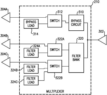
1. A multiplexer configured to support carrier aggregation and non-carrier aggregation, the multiplexer comprising:
a filter bank including a set of filters, at least one filter of the set of filters configured to transmit a signal of a first frequency band and at least one other filter of the set of filters configured to transmit a signal of a second frequency band that differs from the first frequency band;
a load circuit bank including a plurality of load circuits configured to reduce insertion loss in the multiplexer;
a second load circuit bank including a second plurality of load circuits, the second load circuit bank connected to the filter bank;
a switch configured to selectively connect a filter from the filter bank to a load circuit from the second load circuit bank; and
a bypass circuit configured to connect an input port of the multiplexer to an output port of the multiplexer when a control signal received from a baseband processor indicates the multiplexer is to operate in a non-carrier aggregation mode and an input signal is associated with the first frequency band, and connect the input port of the multiplexer to a load circuit of the plurality of load circuits when the control signal indicates the multiplexer is to operate in a carrier aggregation mode.
|