| CPC H04B 1/0017 (2013.01) [H04B 1/1676 (2013.01); H04B 1/62 (2013.01)] | 20 Claims |
|
1. A digital radio frequency (RF) transmitter comprising:
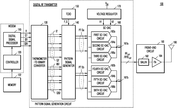
a switched-capacitor digital-to-analog converter (SC-DAC) including,
a first switched-capacitor digital-to-analog converter (SC-DAC) circuit including a plurality of first paths, each including a first amplifier and a first capacitor, the first SC-DAC circuit configured to receive a plurality of first pattern signals in parallel and output a first radio frequency (RF) signal to an output terminal by summing the plurality of first pattern signals,
a second SC-DAC circuit including a plurality of second paths, each including a second amplifier and a second capacitor, the second SC-DAC circuit configured to receive a plurality of second pattern signals in parallel and output a second RF signal to the output terminal by summing the plurality of second pattern signals, and
a third SC-DAC circuit including a plurality of third paths, each including a third amplifier and a third capacitor, the third SC-DAC circuit configured to receive a plurality of third pattern signals in parallel and output a third RF signal to the output terminal by summing the plurality of third pattern signals; and
processing circuitry configured to generate the plurality of first pattern signals, the plurality of second pattern signals, and the plurality of third pattern signals, based on patterns of inphase (I)-quadrature (Q) binary data pairs and patterns of inverted I-Q binary data pairs, the plurality of second pattern signals lagging the plurality of first pattern signals by a first phase, and the plurality of third pattern signals lagging the plurality of first pattern signals by a second phase,
wherein the SC-DAC is configured to remove an n-th harmonic component of an RF analog signal by amplifying the first through third pattern signals to have a certain magnitude ratio and synthesizing the amplified first through third pattern signals into the RF analog signal, where “n” is an integer of at least 3.
|