| CPC H03K 3/037 (2013.01) [G06F 1/12 (2013.01); H03K 19/20 (2013.01)] | 20 Claims |
|
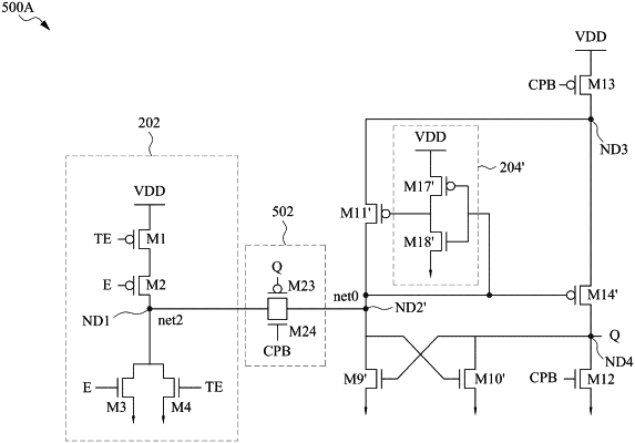
1. A clock gating circuit comprising:
a NOR logic gate coupled to a first node, and being configured to receive a first enable signal and a second enable signal, and to output a first control signal;
a transmission gate coupled between the first node and a second node, the transmission gate being configured to receive the first control signal, an inverted clock input signal and a clock output signal;
a cross-coupled pair of transistors coupled between the second node and an output node, and being configured to receive at least a second control signal; and
a first transistor of a first type, the first transistor including a first gate terminal, a first drain terminal and a first source terminal, the first gate terminal being configured to receive the inverted clock input signal, the first drain terminal being coupled to at least the output node, and the first source terminal being coupled to a reference voltage supply, the first transistor being configured to adjust the clock output signal responsive to the inverted clock input signal.
|