| CPC H03K 17/6872 (2013.01) [H01L 29/2003 (2013.01); H01L 29/7789 (2013.01); H03K 2217/0036 (2013.01)] | 16 Claims |
|
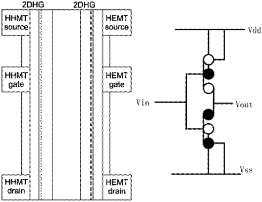
1. A driving circuit, wherein the driving circuit comprises a control module and a driving signal output module, the control module is electrically connected to the driving signal output module, and the driving signal output module is electrically connected to a to-be-driven device,
wherein the driving signal output module comprises at least two transistors, and the at least two transistors are epitaxially grown on the same substrate; and
the control module is configured to control a closed state of the at least two transistors, so as to control an operation state of the to-be-driven device,
wherein,
the at least two transistors comprise at least one P-type transistor and at least one N-type transistor;
the at least two transistors comprise at least one high electron mobility transistor (HEMT) and at least one high hole mobility transistor (HHMT), the substrate comprises a vertical interface, and the HEMT and the HHMT are located at two sides of the vertical interface respectively;
the at least one HEMT and the at least one HHMT each contain a channel layer and a barrier layer, the channel layer is provided outside the vertical interface, the barrier layer is provided outside the channel layer, an interface between the channel layer and the barrier layer comprises a first polar surface and a second polar surface, and the first polar surface and the second polar surface are located at two sides of the vertical interface respectively; and
the first polar surface provides a two-dimensional electron gas, and the second polar surface provides a two-dimensional hole gas.
|