US 11,870,330 B2
Device and method for voltage drop compensation
Jean Camiolo, St. Egreve (FR); and Alexandre Pons, Vizille (FR)
Assigned to STMicroelectronics (Grenoble 2) SAS, Grenoble (FR)
Filed by STMicroelectronics (Grenoble 2) SAS, Grenoble (FR)
Filed on Oct. 6, 2022, as Appl. No. 17/938,489.
Application 17/938,489 is a continuation of application No. 16/906,489, filed on Jun. 19, 2020, granted, now 11,469,677.
Claims priority of application No. 1907196 (FR), filed on Jun. 28, 2019.
Prior Publication US 2023/0029349 A1, Jan. 26, 2023
Int. Cl. H02M 3/335 (2006.01); H02M 1/08 (2006.01)
CPC H02M 3/33553 (2013.01) [H02M 1/08 (2013.01)] 20 Claims
OG exemplary drawing
 
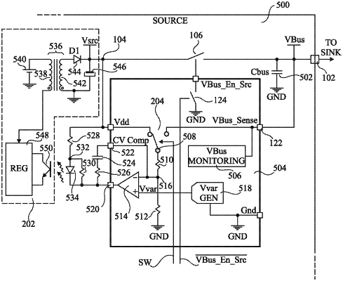
1. A first circuit comprising: a voltage monitoring circuit configured to verify that a bus voltage of an output terminal of a voltage source device is in a correct range; a first switch configured to control a third switch that selectively connects or isolates the output terminal of the voltage source device to or from, respectively, a supply voltage node of a voltage converter; and a second switch configured to mutually-exclusively couple an intermediate node to: the supply voltage node of the voltage converter during a first regulation mode; or the output terminal of the voltage source device during a second regulation mode.