| CPC H01S 5/0264 (2013.01) [H01S 5/0421 (2013.01); H01S 5/04256 (2019.08); H01S 5/12 (2013.01); H01S 5/125 (2013.01); H01S 5/2275 (2013.01)] | 16 Claims |
|
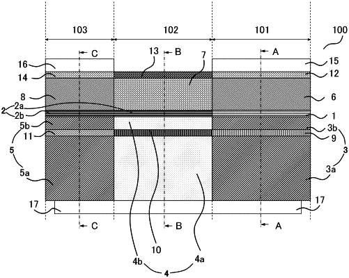
1. A semiconductor laser comprising:
a DFB unit including a back surface side first cladding layer of a first conductivity type, a first diffraction grating layer of a first conductivity type, a light emitting layer having a first MQW structure and emitting a laser beam, a front surface side first cladding layer of a second conductivity type, and a first contact layer of a second conductivity type which are stacked;
a DBR unit including a back surface side second cladding layer having a resistivity higher than that of the back surface side first cladding layer, a second diffraction grating layer reflecting part of the laser beam toward the DFB unit, a first core layer guiding a remnant of the laser beam and having a second MQW structure having an effective bandgap energy smaller than that of the first MQW structure, and a front surface side second cladding layer having a resistivity higher than that of the front surface side first cladding layer which are stacked; and
a PD unit including a back surface side third cladding layer of a first conductivity type, a second core layer having the second MQW structure absorbing the remnant of the laser beam guided by the first core layer of the DBR unit, a front surface side third cladding layer of a second conductivity type, and a second contact layer of a second conductivity type which are stacked.
|