| CPC H01Q 9/0414 (2013.01) [H01L 21/4853 (2013.01); H01L 21/4857 (2013.01); H01L 21/563 (2013.01); H01L 23/49816 (2013.01); H01L 23/49822 (2013.01); H01L 23/49838 (2013.01); H01L 23/66 (2013.01); H01L 2223/6616 (2013.01); H01L 2223/6677 (2013.01)] | 25 Claims |
|
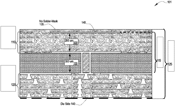
1. An electronic assembly, comprising:
a first region, including:
a first antenna patch,
a second antenna patch, and
multiple first metal portions coplanar with the first antenna patch;
multiple second metal portions coplanar with the second antenna patch;
multiple third metal portions, wherein individual ones of the third metal portions are between a corresponding individual one of the first metal portions and a corresponding one of the second metal portions;
a second region including a conductive structure, wherein the conductive structure includes a first conductive via; and
a third region between the first region and the second region, wherein the third region includes a second conductive via in conductive contact with the conductive structure and with the first antenna patch.
|