| CPC H01Q 3/30 (2013.01) [H01Q 9/0414 (2013.01)] | 20 Claims |
|
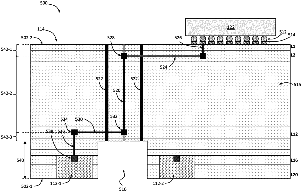
1. An antenna assembly, comprising:
a printed circuit board (PCB) having a first face and an opposing second face;
a first antenna element and a second antenna element at the first face of the PCB;
a recess in the first face of the PCB, between the first antenna element and the second antenna element; and
a conductive via in the PCB, the conductive via having a first end at the second face of the PCB and having a second end abutting the recess,
wherein:
a footprint of the conductive via is within a footprint of the recess,
the PCB includes a first conductive line in a first layer of the PCB and a second conductive line in a second layer of the PCB,
the first conductive line is between the second face of the PCB and the second layer of the PCB,
the first conductive line is coupled to a first point of the conductive via and further coupled to a conductive contact at the second face of the PCB to be coupled to a beamformer die, and
the second conductive line is coupled to a second point of the conductive via and further coupled to the first antenna element.
|