| CPC H01Q 1/2283 (2013.01) [H01L 21/486 (2013.01); H01L 21/4853 (2013.01); H01L 21/4857 (2013.01); H01L 23/49816 (2013.01); H01L 23/66 (2013.01); H01L 2223/6677 (2013.01)] | 20 Claims |
|
1. A semiconductor device comprising:
a semiconductor die comprising a radio frequency (RF) circuit;
a first dielectric layer disposed over a first surface of the semiconductor die;
an antenna layer disposed over a surface of the first dielectric layer; and
an antenna feeding structure coupling the antenna layer to the RF circuit of the semiconductor die, wherein:
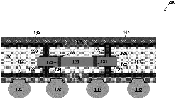
the semiconductor die comprises an opening; and
the antenna feeding structure comprises:
a first portion comprising a first via arranged within the opening of the semiconductor die and extending to the first surface of the semiconductor die,
a second portion comprising a second via arranged through the first dielectric layer and extending from the first surface of the semiconductor die to the antenna layer, and
a third portion comprising a planar conductive feature disposed on the first surface of the semiconductor die, the third portion conductively connecting the first portion to the second portion.
|