| CPC H01L 33/62 (2013.01) [H01L 25/0753 (2013.01); H01L 27/1259 (2013.01); H01L 29/78633 (2013.01); G09G 3/32 (2013.01); G09G 2300/0426 (2013.01); G09G 2300/0439 (2013.01); G09G 2300/08 (2013.01); G09G 2310/0267 (2013.01); H01L 2933/0066 (2013.01)] | 15 Claims |
|
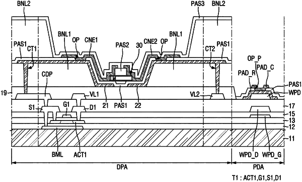
1. A display device comprising:
a first substrate comprising a display area and a pad area;
a wire pad on the first substrate in the pad area;
electrodes on the display area and spaced from each other;
a pad electrode base layer directly on the wire pad, having a greater width than the wire pad, and covering sides of the wire pad;
light-emitting elements on the electrodes in the display area; and
a pad electrode upper layer in the pad area and contacting the pad electrode base layer,
wherein the pad electrode base layer comprises a same material as the electrodes.
|