| CPC H01L 33/54 (2013.01) [G09G 3/20 (2013.01); H01L 33/56 (2013.01); H10K 19/00 (2023.02); H10K 50/80 (2023.02); G09G 2320/028 (2013.01); G09G 2320/068 (2013.01)] | 18 Claims |
|
1. A display device, comprising:
a substrate;
a first light emitting element disposed on the substrate;
a second light emitting element disposed on the substrate and positioned adjacent to the first light emitting element;
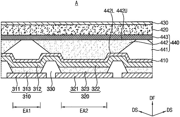
a first encapsulation layer disposed on the first light emitting element and the second light emitting element; and
a light path control layer disposed on the first encapsulation layer, the light path control layer including a first pattern overlapping the first light emitting element and having a first refractive index and a second pattern overlapping the second light emitting element and having a second refractive index that is greater than the first refractive index, wherein an emission area of the second light emitting element is a different size from that of an emission area of the first light emitting element,
wherein the first pattern does not overlap the second light emitting element, and
wherein the light path control layer further includes a capping layer directly disposed on the first pattern,
wherein the second pattern includes a first side surface and a second side surface opposite to the first side surface, wherein each of the first side surface and the second side surface is slanted with respect to an upper surface of the first encapsulation layer, wherein each of the first side surface and the second side surface extends from a bottom surface of the capping layer to the upper surface of the first encapsulation layer and contacts the capping layer and the first encapsulation layer.
|