| CPC H01L 33/285 (2013.01) [H01L 25/0756 (2013.01)] | 20 Claims |
|
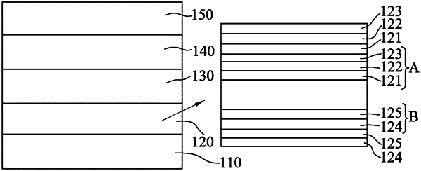
1. A light-emitting diode, comprising:
an N-type cladding layer;
a superlattice structure disposed on said N-type cladding layer;
an active layer directly disposed on said superlattice structure;
a P-type electron-blocking layer disposed on said active layer; and
a P-type cladding layer disposed on said P-type electron-blocking layer,
wherein:
said superlattice structure includes a first superlattice unit that contains at least one first layered element, said first layered element having a sub-layer which is made of a nitride-based semiconductor material including Al, and which has an energy band gap greater than that of said electron-blocking layer;
said P-type electron-blocking layer is made of a nitride-based semiconductor material including Al, and has an energy band gap greater than that of said P-type cladding layer.
|