| CPC H01L 33/24 (2013.01) [H01L 33/382 (2013.01); H01L 33/405 (2013.01); H01L 33/46 (2013.01); H01L 33/22 (2013.01); H01L 33/32 (2013.01)] | 22 Claims |
|
1. A light emitting diode (LED) chip, comprising:
an n-type layer;
a p-type layer;
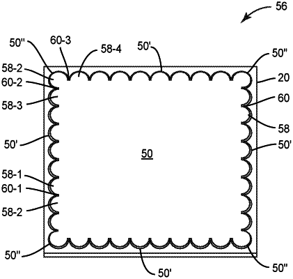
an active layer arranged between the n-type layer and the p-type layer, wherein the p-type layer, the active layer, and a portion of the n-type layer form an active LED structure mesa with at least one mesa sidewall, wherein the at least one mesa sidewall forms a shape with a repeating pattern along only a first portion of the at least one mesa sidewall such that a second portion of the at least one mesa sidewall is devoid of any repeating pattern; and
a reflective structure on the active LED structure mesa and on the at least one mesa sidewall, wherein the reflective structure is arranged to cover the repeating pattern.
|