| CPC H01L 31/1864 (2013.01) [H01L 31/02963 (2013.01); H01L 31/06 (2013.01); H01L 31/073 (2013.01)] | 20 Claims |

|
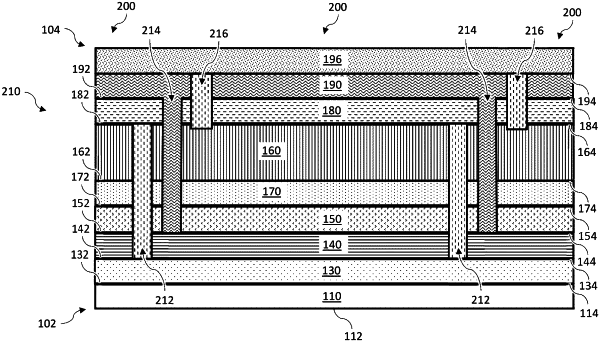
1. A method of treating a fully-formed photovoltaic device disconnected from a load to form an open circuit, the device having an absorber layer comprising a group II-VI p-type semiconductor material doped with an element from group IB, the method comprising:
heating at least a portion of the absorber layer of the photovoltaic device to a temperature in a range of 200 C to 1000 C for a duration of up to 60 seconds to promote at least one dopant chemical reaction in the absorber layer; and
quenching the at least one dopant chemical reaction by ending the heating and allowing the absorber layer of the photovoltaic device to cool, whereby the absorber layer reaches a temperature below 100 C within 120 seconds after initiating the heating step,
wherein the absorber layer comprises cadmium and tellurium and is doped with copper and chlorine, and the heating promotes dissociation of Cli—CuCd complexes.
|