| CPC H01L 31/02322 (2013.01) [G01B 7/003 (2013.01); G06F 3/042 (2013.01); G06F 3/0412 (2013.01); H01L 31/1136 (2013.01)] | 17 Claims |
|
1. A display panel, comprising a plurality of light-sensing areas arranged in an array manner, wherein the display panel comprises:
an upconversion material layer, wherein the upconversion material layer is configured to absorb interactive light emitted from an interactive light source and convert the interactive light from a first wave band into a second wave band, and the second wave band is less than the first wave band;
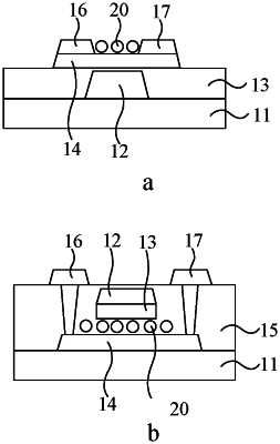
a light-sensing circuit, wherein the light-sensing circuit is disposed in the plurality of light-sensing areas and comprises a light-sensing transistor, the light-sensing transistor comprises a substrate, a metal oxide active layer, a gate insulating layer, a gate layer, and a source/drain layer, the upconversion material layer is disposed between the interactive light source and the metal oxide active layer, the second wave band is within an absorption band of the metal oxide active layer, and the light-sensing transistor is configured to convert a light intensity signal of the interactive light into an electrical signal, wherein the substrate, the gate insulating layer, and the source/drain layer, which are stacked, one of the gate layer or the metal oxide active layer is disposed between the substrate and the gate insulating layer, and the other is disposed between the gate insulating layer and the source/drain layer, wherein the upconversion material layer is disposed in the light-sensing transistor and is disposed on a side of the metal oxide active layer away from the substrate; and
a position-detecting circuit, wherein the position-detecting circuit is electrically connected to the light-sensing circuit and is configured to identify a position where the interactive light is irradiated.
|