| CPC H01L 29/8611 (2013.01) [H01L 29/66128 (2013.01); H01L 29/66136 (2013.01)] | 13 Claims |
|
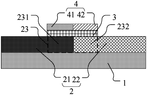
1. A semiconductor device, comprising:
a substrate;
a semiconductor structure positioned on a side of the substrate, the semiconductor structure comprising a first semiconductor structure and a second semiconductor structure, the first semiconductor structure and the second semiconductor structure forming a PN junction;
an insulating layer, positioned on a side of the semiconductor structure facing away from the substrate; and
a conductive layer positioned on a side of the insulating layer facing away from the substrate, an orthographic projection of the conductive layer on the substrate at least partially overlapping an orthographic projection of the PN junction on the substrate;
wherein the conductive layer is configured to reduce a potential barrier of the PN junction formed by the first semiconductor structure and the second semiconductor structure;
wherein the conductive layer comprises a first conductive layer and a second conductive layer, the first conductive layer is a polysilicon conductor doped with a P-type ion, and the second conductive layer is a polysilicon conductor doped with an N-type ion.
|