| CPC H01L 29/8086 (2013.01) [H01L 21/02576 (2013.01); H01L 21/02579 (2013.01); H01L 29/0661 (2013.01); H01L 29/0665 (2013.01); H01L 29/0847 (2013.01); H01L 29/1045 (2013.01); H01L 29/1066 (2013.01)] | 14 Claims |
|
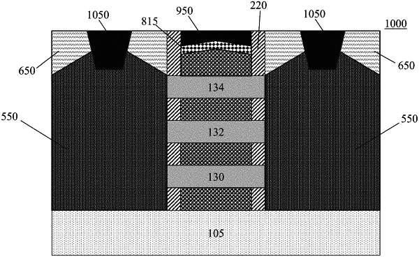
1. A Junction Field Effect Transistor (JFET) comprising:
a substrate;
a source disposed on the substrate, the source having an S/D doping, the S/D doping having an S/D doping type;
a drain disposed on the substrate, the drain having the S/D doping type;
two or more channels electrically connected in parallel between the source and drain and capable of carrying a current between the source and drain, each of the channels having two or more channel surfaces, the channel having a channel doping with a channel doping type, the channel doping type being the same as the S/D doping type, where the channels are made of nanosheet layers and a channel layer thickness is between 5 nanometers (nm) and 30 nm;
a first gate in direct contact with a first channel surface, the first gate having a gate doping with a gate doping type, the gate doping type being an opposite doping to the channel doping type;
one or more second gates each in direct contact with a respective second channel surface, the second gates being doped with the gate doping type,
gate spacers spaced lateral from the first and second gates;
wherein the first and second gates are electrically connected so a voltage applied to the first and second gates creates at least two depletion regions in each of the channels, a first depletion region of the at least two depletion regions being on one or more of the first channel surfaces and a second depletion region of the at least two depletion regions being on one or more of the second channel surfaces;
where: the first gate and the one or more second gates form an all-around gate of a single unified structure; and
wherein an outermost one of the first and second gates has an outermost point that does not extend as far outward as an outermost point of the source, an outermost point of the drain, and an outermost point of the gate spacers.
|