| CPC H01L 29/7869 (2013.01) [H01L 29/24 (2013.01); H01L 29/66742 (2013.01); H10B 12/05 (2023.02); H10B 12/31 (2023.02)] | 9 Claims |
|
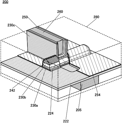
1. A semiconductor device comprising a transistor, the transistor comprising:
a first insulator;
a second insulator over the first insulator;
a first oxide over the second insulator;
a second oxide over the first oxide;
a third oxide over the second oxide;
a first conductor and a second conductor over the second oxide;
a third insulator over the third oxide; and
a third conductor over the third insulator;
wherein in a channel width direction of the transistor, with reference to a height of a bottom surface of the first insulator, a height of a bottom surface of the third conductor in a region where the third conductor and the second oxide do not overlap with each other is lower than a height of a bottom surface of the second oxide, and
wherein in the channel width direction of the transistor, at least part of the third oxide in a region where the third oxide and the second oxide do not overlap with each other is in contact with the first insulator.
|