| CPC H01L 29/7853 (2013.01) [H01L 29/0673 (2013.01); H01L 29/1037 (2013.01); H01L 29/1054 (2013.01); H01L 29/6653 (2013.01); H01L 29/6681 (2013.01); H01L 29/66818 (2013.01); H01L 29/7855 (2013.01); H01L 21/02238 (2013.01); H01L 21/02241 (2013.01); H01L 21/31111 (2013.01); H01L 21/31122 (2013.01); H01L 29/165 (2013.01); H01L 29/205 (2013.01); H01L 29/42392 (2013.01)] | 15 Claims |
|
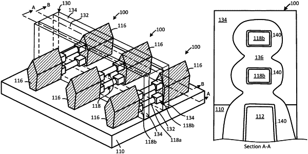
1. A semiconductor structure comprising:
a body comprising a semiconductor material;
a subfin beneath the body;
a gate structure wrapped around the body, and the gate structure on a top and along sidewalls of the subfin, the gate structure including a gate electrode and a gate dielectric between the body and the gate electrode, and the gate structure including a gate spacer; and
a source region and a drain region, the body being between the source and drain regions; wherein the body has a first cross-sectional shape under the gate dielectric and a second cross-sectional shape under the gate spacer, wherein the first cross-sectional shape is more rounded than the second cross-sectional shape, and wherein the gate spacer extends vertically beneath the second cross-sectional shape.
|