| CPC H01L 29/78391 (2014.09) [G11C 11/223 (2013.01); G11C 11/2273 (2013.01); G11C 11/2275 (2013.01); H01L 29/6684 (2013.01); H10B 51/30 (2023.02)] | 20 Claims |
|
1. A ferroelectric field-effect transistor (FeFET) configured as a 2-bit storage device, the FeFET comprising:
a semiconductor substrate including:
a source region in the semiconductor substrate; and
a drain region in the semiconductor substrate;
a gate stack over the semiconductor substrate, with the source region and the drain region extending to opposite sides of the gate stack, the gate stack including:
a ferroelectric layer over the semiconductor substrate;
a gate region over the ferroelectric layer; and
wherein:
first and second ends of the ferroelectric layer are proximal correspondingly to the source and drain regions; and
the ferroelectric layer includes dipoles; and
a first set of dipoles at the first end of the ferroelectric layer has a first polarization; and
a second set of dipoles at the second end of the ferroelectric layer has a second polarization, the second polarization being substantially opposite of the first polarization, the first and second polarizations of the corresponding first and second sets of dipoles representing storage of 2 bits, wherein:
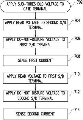
a first bit of the 2-bit storage device being configured to be read by application of a read voltage to the source region and a do-not-disturb voltage to the drain region; and
a second bit of the 2-bit storage device being configured to be read by application of the do-not-disturb voltage to the source region and the read voltage to the drain region.
|