| CPC H01L 29/7825 (2013.01) [H01L 29/7806 (2013.01); H01L 29/7839 (2013.01)] | 11 Claims |
|
1. A semiconductor device, comprising:
a semiconductor substrate;
an epitaxial layer disposed on said semiconductor substrate;
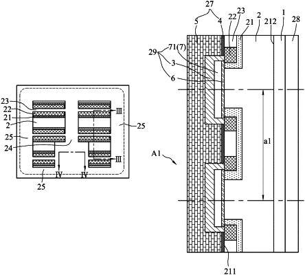
a cell zone including a plurality of unit cells disposed in said epitaxial layer opposite to said semiconductor substrate, each of said unit cells including a well region having a first conductive type, a source region having a second conductive type and disposed in said well region, and a well contact region having the first conductive type and extending through said source region to contact said well region;
a transition zone surrounding said cell zone and having a doped region which has the first conductive type and which is disposed in said epitaxial layer opposite to said semiconductor substrate and is directly connected to said well contact region of at least one of said unit cells;
a source electrode unit disposed on said epitaxial layer opposite to said semiconductor substrate and including a first portion and a second portion connected to said first portion; and
a plurality of gate electrode units, each of which is disposed on said epitaxial layer opposite to said semiconductor substrate and extends between two adjacent ones of said unit cells to cover a portion of said source region of each of said adjacent ones of said unit cells,
wherein said first portion of said source electrode unit is electrically connected to said well contact region and a portion of said source region of each of said unit cells, and
wherein said second portion of said source electrode unit is electrically connected to said doped region of said transition zone.
|