| CPC H01L 29/781 (2013.01) [H01L 29/1095 (2013.01); H01L 29/401 (2013.01); H01L 29/407 (2013.01); H01L 29/66734 (2013.01); H01L 29/7813 (2013.01)] | 20 Claims |
|
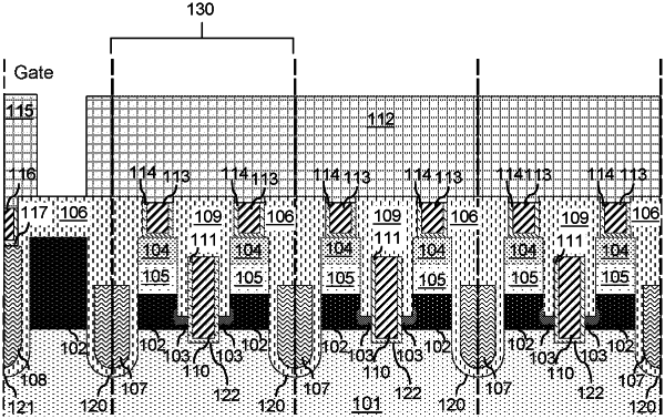
1. An inverted field-effect-transistor (iT-FET) semiconductor device, comprising a source layer on a bottom and a drain metal disposed on a top of a semiconductor substrate:
a vertical current conducting channel between said source layer and said drain metal controlled by a trench gate electrode disposed in a gate trench lined with an insulating material;
a heavily doped drain region disposed near the top of the substrate surrounding an upper portion of a shield trench and the gate trench;
a doped body region disposed in the substrate and surrounding a lower portion of the shield trench;
a shield electrode extending upward from the source layer in the shield trench electrically shorting the source layer and the body region, wherein the shield electrode extends upward to the heavily doped drain region and is insulated from the heavily doped drain region.
|