| CPC H01L 29/7802 (2013.01) [H01L 21/265 (2013.01); H01L 21/31053 (2013.01); H01L 21/765 (2013.01); H01L 21/76224 (2013.01); H01L 21/823487 (2013.01); H01L 29/0634 (2013.01); H01L 29/402 (2013.01)] | 13 Claims |
|
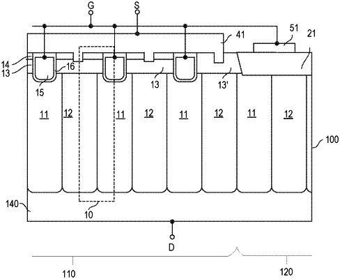
1. A method, comprising:
forming a trench in a first surface in an edge region of a semiconductor body;
forming a plurality of superjunction transistor cells in an inner region of a semiconductor body; and
forming an insulation layer on the first surface of the semiconductor body in the edge region and in the inner region,
wherein forming the insulation layer comprises a thermal oxidation process,
wherein forming the plurality of superjunction transistor cells comprises implanting dopant atoms in the inner region before forming the trench,
wherein implanting the dopant atoms comprises forming a plurality of first implanted regions one above the other in the semiconductor body and forming a plurality of second implanted regions one above the other in the semiconductor body,
wherein the first implanted regions include dopant atoms of a first doping type,
wherein the second implanted regions include dopant atoms of a second doping type complementary to the first doping type, and
wherein forming the insulation layer diffuses and activates the first type dopant atoms included in the first implanted regions and the second type dopant atoms included in the second implanted regions, thereby forming super junction structures of the superjunction transistor cells.
|