| CPC H01L 29/42392 (2013.01) [H01L 21/28185 (2013.01); H01L 21/3115 (2013.01); H01L 21/823412 (2013.01); H01L 21/823431 (2013.01); H01L 21/823437 (2013.01); H01L 21/823462 (2013.01); H01L 27/0886 (2013.01); H01L 29/0665 (2013.01); H01L 29/513 (2013.01); H01L 29/78696 (2013.01)] | 20 Claims |
|
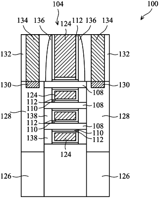
8. A method, comprising:
forming a plurality of first semiconductor nanosheets corresponding to channel regions of a first gate all around transistor;
forming a plurality of second semiconductor nanosheets corresponding to channel regions of a second gate all around transistor;
depositing an interfacial dielectric layer on the first and second semiconductor nanosheets;
depositing a high-K dielectric layer on the interfacial dielectric layer;
depositing a cap layer on the high-K dielectric layer;
removing the cap layer from the high-K dielectric layer on the second semiconductor nanosheets; and
diffusing metal atoms from the cap layer into the interfacial dielectric layer on the first semiconductor nanosheets by performing a thermal annealing process after removing the cap layer from the high-K dielectric layer on the second semiconductor nanosheets.
|