| CPC H01L 29/42392 (2013.01) [H01L 29/0665 (2013.01); H01L 29/0673 (2013.01); H01L 29/1037 (2013.01); H01L 29/401 (2013.01); H01L 29/6653 (2013.01); H01L 29/66545 (2013.01); H01L 29/78696 (2013.01)] | 20 Claims |

|
1. A method, comprising:
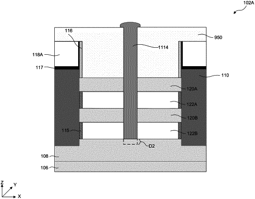
forming a superlattice structure with first and second nanostructured layers arranged in an alternating configuration on a substrate;
forming a source/drain (S/D) region on the substrate;
forming a nanostructured region through the superlattice structure;
forming a gate structure surrounding the nanostructured region about a first axis and surrounding the first nanostructured layers about a second axis different from the first axis; and
forming contact structures on the S/D region and the gate structure.
|