| CPC H01L 29/42364 (2013.01) [H01L 21/28238 (2013.01); H01L 29/0653 (2013.01)] | 3 Claims |
|
1. A method for fabricating a high-voltage transistor device, comprising:
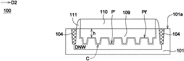
providing a semiconductor substrate;
etching a portion of the semiconductor substrate using a first patterned mask to form a plurality of grooves extending downward from a surface of the semiconductor substrate to form a sawtooth sectional profile;
forming an isolation structure, on an outside of the plurality of grooves, and extending from the surface downwards into the semiconductor substrate to defining a high-voltage area;
etching another portion of the semiconductor substrate in the high-voltage area using a second patterned mask;
forming a gate dielectric layer, on the high-voltage area and partially filled in the plurality of grooves and contacting to a bottom of the plurality of grooves;
forming a gate, on the gate dielectric layer;
forming a source region, in the semiconductor substrate; and
forming a drain region, in the semiconductor substrate and isolated from the source region.
|