| CPC H01L 29/4236 (2013.01) [H01L 21/02057 (2013.01); H01L 29/0847 (2013.01); H01L 29/401 (2013.01); H01L 29/66621 (2013.01)] | 13 Claims |
|
1. A method for forming a semiconductor structure, comprising:
providing a substrate;
forming an active region on the substrate;
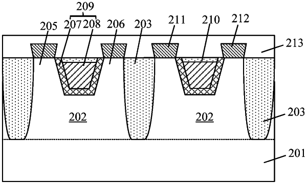
forming at least one trench in the active region, the at least one trench at least dividing the active region into a source region on one side of the at least one trench and a drain region on another side of the at least one trench;
forming a gate structure in the at least one trench; and
forming an elevated source region and an elevated drain region on the source region and the drain region, respectively;
wherein a bottom width of the elevated source region is equal to a top width of the source region, and a bottom width of the elevated drain region is equal to a top width of the drain region;
a top width of the elevated source region is greater than the bottom width of the elevated source region, and a top width of the elevated drain region is greater than the bottom width of the elevated drain region, and an opening size of the at least one trench is greater than the bottom width of the elevated source region or the bottom width of the elevated drain region.
|