| CPC H01L 29/42328 (2013.01) [H01L 21/26513 (2013.01); H01L 21/32139 (2013.01); H01L 23/528 (2013.01); H01L 23/5226 (2013.01); H01L 29/401 (2013.01); H01L 29/40114 (2019.08); H01L 29/66825 (2013.01); H01L 29/7881 (2013.01)] | 20 Claims |
|
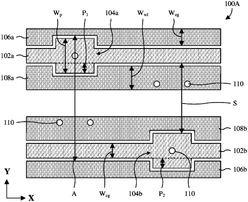
1. A method for forming an integrated chip, the method comprising:
forming a first control-gate stack and a second control-gate stack elongated in parallel with a first axis, wherein the first control-gate stack has a first protrusion protruding towards the second control-gate stack from a first sidewall of the first control-pate stack and has a second protrusion protruding away from the second control-gate stack from a second sidewall of the first control-pate stack, and wherein the first and second protrusions define a pad, overlap with and protrude along a second axis orthogonal to the first axis;
depositing a gate layer over the first and second control-gate stacks; and
patterning the gate layer to form an erase gate and a word line respectively on opposite sides of the first control-gate stack, wherein a sidewall of the word line has a first indent receiving and conforming to the first protrusion, and
wherein a sidewall of the erase gate has a second indent receiving and conforming to the second protrusion; wherein the pad is between the erase gate and the word line along the second axis, wherein the first sidewall of the first control-pate stack faces and borders the sidewall of the word line, wherein the second sidewall of the first control-pate stack faces and borders the sidewall of the erase pate, and wherein the first and second sidewalls of the first control-pate stack extend linearly and continuously from the pad to a second pad with a constant separation between the first and second sidewalls.
|