| CPC H01L 29/404 (2013.01) [H01L 29/1608 (2013.01)] | 31 Claims |
|
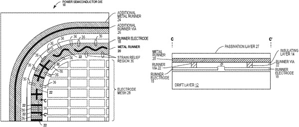
1. A semiconductor device comprising:
a drift layer that includes an active region;
a runner electrode on the drift layer that extends along a runner electrode path;
and
a runner electrode strain relief region that comprises a closed region in which electrically conductive material is not provided that is surrounded by the runner electrode when the runner electrode is viewed from above.
|