| CPC H01L 29/2003 (2013.01) [H01L 21/0262 (2013.01); H01L 21/02389 (2013.01); H01L 21/02458 (2013.01)] | 11 Claims |
|
1. A method comprising:
providing a precursor package having a plurality of switch dies, a package substrate, and a first mold compound, wherein:
the package substrate includes a plurality of module substrates, wherein an inter-module area is in between two adjacent module substrates of the plurality of module substrates;
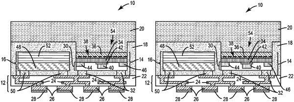
each of the plurality of switch dies resides over a corresponding module substrate, and comprises an electrode region, a plurality of switch interconnects extending from a bottom surface of the electrode region to the corresponding module substrate, an aluminium gallium nitride (AlGaN) barrier layer over a top surface of the electrode region, a gallium nitride (GaN) buffer layer over the AlGaN barrier layer, a lateral two-dimensional electron gas (2DEG) layer realized at a heterojunction of the AlGaN barrier layer and the GaN buffer layer, and a silicon switch substrate over the GaN buffer layer; and
the first mold compound encapsulates side surfaces of each of the plurality of switch dies, wherein a top surface of the silicon switch substrate of each of the plurality of switch dies is exposed;
removing substantially the silicon switch substrate of each of the plurality of switch dies to provide a plurality of thinned switch dies and form an opening over each of the plurality of thinned switch dies, wherein a top surface of each of the plurality of thinned switch dies is exposed at a bottom of the opening;
applying a second mold compound to substantially fill each opening to form a GaN based package; and
singulating the GaN based package at each inter-module area to provide a plurality of GaN based modules, wherein each of the plurality of GaN based modules includes one module substrate and at least one thinned switch die.
|