| CPC H01L 29/2003 (2013.01) [H01L 21/02304 (2013.01); H01L 21/0415 (2013.01); H01L 29/0615 (2013.01); H01L 29/1066 (2013.01); H01L 29/7783 (2013.01); H01L 29/7787 (2013.01)] | 18 Claims |
|
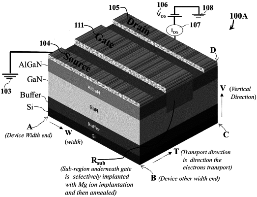
1. A field effect transistor, comprising:
a source;
a gate;
a drain;
a semiconductor region under the source, the gate and the drain, such that the semiconductor region includes a gallium nitride (GaN) layer and a three nitride (III-N) layer; and
a sub-region of the semiconductor region underneath the gate doped with Mg ions at selective locations in the sub-region, wherein each of the selective locations doped with Mg ions in the sub-region has a profile, such that the profile includes a vertical profile length and a profile width, and wherein the profiles form a pattern, such that profile widths of the profiles increase along a direction from a first width end to a second width end of the field effect transistor.
|