| CPC H01L 29/1608 (2013.01) [H01L 29/0619 (2013.01); H01L 29/872 (2013.01); H01L 29/8725 (2013.01)] | 7 Claims |
|
1. A silicon carbide semiconductor device, comprising:
a first silicon carbide semiconductor layer, having a first conductivity type;
a second silicon carbide semiconductor layer, having the first conductivity type and disposed on the first silicon carbide semiconductor layer;
a third silicon carbide semiconductor layer, having a second conductivity type and disposed on an upper surface of the second silicon carbide semiconductor layer;
a first semiconductor region, having the first conductivity type and disposed in the third silicon carbide semiconductor layer;
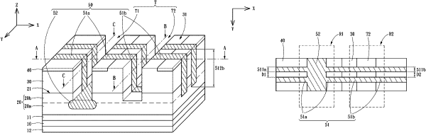
a first trench, perpendicularly penetrating through the first semiconductor region and the third silicon carbide semiconductor layer into the second silicon carbide semiconductor layer and extending in a first horizontal direction;
a second trench, spaced apart from the first trench, the second trench perpendicularly penetrating through the third silicon carbide semiconductor layer into the second silicon carbide semiconductor layer and extending in the first horizontal direction;
a second semiconductor region, having the second conductivity type and comprising a plurality of first portions extending in a second horizontal direction and a second portion extending in the first horizontal direction and disposed in the second silicon carbide semiconductor layer under the first trench;
a gate region, comprising a gate insulating layer disposed in the first trench and a poly gate embedded in the first trench and formed on the gate insulating layer; and
a metal electrode, in contact with the first semiconductor region and the gate region and embedded in the second trench to be in electrical contact with the second semiconductor region and the third silicon carbide semiconductor layer, wherein a side wall and a bottom wall of the metal electrode forms a Schottky junction with the second silicon carbide semiconductor layer in the second trench;
wherein the first portion of the second semiconductor region comprises a plurality of pickup regions and a plurality of slice regions, the plurality of pickup regions surrounds the first trench and is connected to the second portion, the plurality of slice regions surrounds the second trench and is connected to the pickup regions, and current flowing from the metal electrode is restricted between the plurality of slice regions which are adjacent.
|