| CPC H01L 29/0817 (2013.01) [H01L 21/26586 (2013.01); H01L 29/66272 (2013.01); H01L 29/732 (2013.01); H01L 29/7371 (2013.01)] | 18 Claims |
|
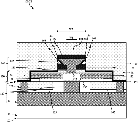
1. A semiconductor structure comprising:
a dielectric layer;
an emitter region comprising:
a first emitter portion extending through the dielectric layer; and
a second emitter portion on the first emitter portion and further extending laterally onto the dielectric layer;
an additional dielectric layer on the second emitter portion;
a base region comprising a first base portion and second base portions, wherein the first base portion is positioned laterally between the second base portions; and
an isolation layer on the base region, the isolation layer including a first isolation portion on the first base portion and second isolation portions on the second base portions, wherein the dielectric layer is on the first isolation portion of the isolation layer and aligned above the first base portion, and wherein the first emitter portion extends through the dielectric layer and the first isolation portion of the isolation layer to the first base portion,
wherein the dielectric layer, the second emitter portion, and the additional dielectric layer are wider than the first emitter portion, and
wherein at least a section of the second emitter portion is narrower than the dielectric layer and the additional dielectric layer.
|