| CPC H01L 29/0673 (2013.01) [H01L 21/30604 (2013.01); H01L 21/3105 (2013.01); H01L 21/31155 (2013.01); H01L 29/0847 (2013.01); H01L 29/42392 (2013.01); H01L 29/66545 (2013.01); H01L 29/66553 (2013.01); H01L 29/78 (2013.01); H01L 29/78696 (2013.01); B82Y 40/00 (2013.01)] | 10 Claims |
|
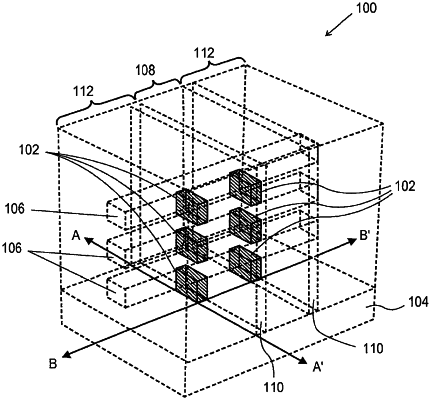
1. A semiconductor device comprising:
a nanowire stack disposed above a substrate, the nanowire stack including vertically-stacked nanowires;
a gate structure wrapped around each of the nanowires to define a channel region of the device, the gate structure including gate sidewalls;
a pair of source/drain regions on opposite sides of the channel region;
a first internal spacer arranged along at least a portion of one of the gate sidewalls between two adjacent ones of the nanowires; and
second internal spacers arranged along respective gate sidewalls underneath a bottommost nanowire in the nanowire stack.
|