| CPC H01L 28/92 (2013.01) [H01L 28/75 (2013.01); H01L 28/91 (2013.01); H10B 12/033 (2023.02); H10B 12/315 (2023.02)] | 20 Claims |
|
1. A manufacturing method of a capacitive structure, comprising:
providing a semiconductor base;
forming a first mask layer on the semiconductor base, and forming a plurality of first round hole patterns distributed uniformly on the first mask layer;
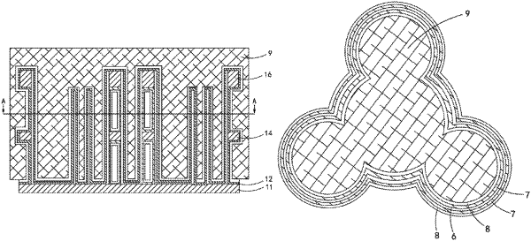
forming first openings distributed uniformly on the semiconductor base by etching based on the first round hole patterns, each of the first openings having a first round projection on the semiconductor base;
forming a second mask layer on one side, away from the semiconductor base, of the first openings, and forming a plurality of second round hole patterns on the second mask layer;
forming second openings distributed uniformly on the semiconductor base by etching based on the second round hole patterns, and meanwhile continuously etching the first openings, so that the first openings and the second openings are same in depth, each of the second openings having a second round projection on the semiconductor base;
wherein a contour line of the second round projection respectively intersects with contours lines of three first round projections;
etching the first openings and the second openings to form capacitive holes; and
depositing a lower electrode layer, a dielectric layer and an upper electrode layer within the capacitive holes to form the capacitive structure.
|