| CPC H01L 28/91 (2013.01) [H01L 28/92 (2013.01); H10B 12/31 (2023.02)] | 15 Claims |
|
1. A method of forming a semiconductor structure, comprising:
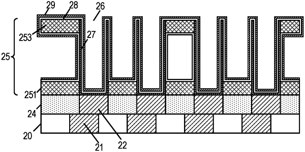
forming a substrate, wherein a plurality of capacitive contacts are provided in the substrate, a plurality of electrically conductive contact pads are provided at a surface of the substrate to be correspondingly connected to a plurality of capacitive contacts on a one to one basis, and a space is present between every two adjacent electrically conductive contact pads;
forming a filling layer that is fully filled in the space;
forming a stacked structure at the filling layer and a surface of the electrically conductive contact pads, wherein the stacked structure includes a plurality of supporting layers stacked one on another along a direction perpendicular to the substrate, the filling layer is in contact with the one supporting layer disposed at a bottom of the stacked structure, and an etching selection ratio between the filling layer and the supporting layer in contact therewith is greater than a preset value; and
etching the stacked structure to form a capacitance hole that runs through the stacked structure and exposes the electrically conductive contact pads.
|