| CPC H01L 28/91 (2013.01) [H01L 21/32139 (2013.01); H01L 28/92 (2013.01); H10B 12/03 (2023.02)] | 14 Claims |
|
1. A method for forming a semiconductor structure, comprising:
forming a stacked structure on a surface of a substrate, capacitor contacts being arranged in the substrate, and the stacked structure comprising supporting layers and sacrificial layers which are alternately stacked along a direction perpendicular to the substrate wherein the forming the stacked structure on the surface of the substrate comprises:
providing the substrate; and
depositing a first supporting layer, a first sacrificial layer, a second supporting layer, a second sacrificial layer, and a third supporting layer in sequence along the direction perpendicular to the substrate;
forming a buffer layer on a surface of the third supporting layer facing away from the substrate;
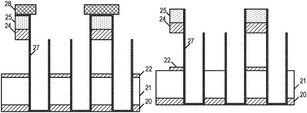
forming capacitor holes penetrating through the stacked structure and the buffer layer and exposing the capacitor contacts;
forming a first electrode layer covering side walls and bottom walls of the capacitor holes and a surface of the buffer layer facing away from the third supporting layer and contacting with the capacitor contacts;
forming a mask layer on a surface of the first electrode layer which is located on the surface of the buffer layer facing away from the third supporting layer, such that the capacitor holes are sealed, wherein an etching pattern exposing the first electrode layer is arranged in the mask layer;
forming an etching window penetrating through the buffer layer and exposing the third supporting layer, by etching the first electrode layer and the buffer layer in sequence along the etching pattern;
removing part of the supporting layers and all of the sacrificial layers in the stacked structure along the etching window;
removing the buffer layer after the removing part of the supporting layers and all of the sacrificial layers such that the first electrode layer protrudes over a residual stacked structure; and
forming a dielectric layer covering the surface of the first electrode layer and a surface of the residual stacked structure, and a second electrode layer covering a surface of the dielectric layer, to form a capacitor.
|