| CPC H01L 28/56 (2013.01) [H01L 21/022 (2013.01); H01L 21/0228 (2013.01); H01L 21/02181 (2013.01); H01L 21/02189 (2013.01); H01L 21/02321 (2013.01)] | 8 Claims |
|
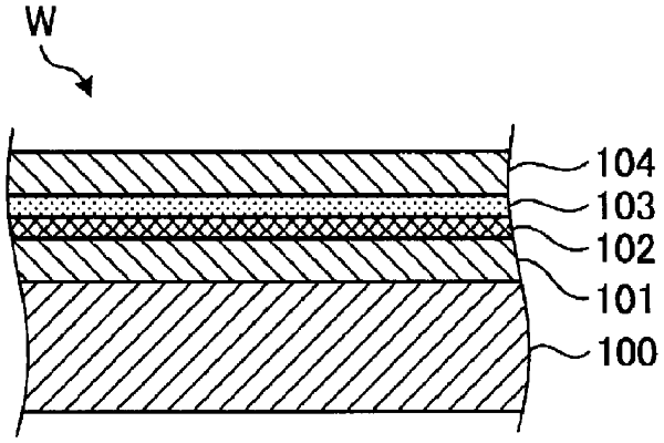
1. A method of manufacturing a semiconductor device, the method comprising:
a first laminating step of laminating a first electrode film on a substrate;
a second laminating step of laminating a capacitive insulator on the first electrode film;
a third laminating step of laminating a metal oxide on the capacitive insulator;
a first annealing step of annealing the first electrode film, the capacitive insulator, and the metal oxide, which are laminated on the substrate; and
a fourth laminating step of laminating a second electrode film on the annealed metal oxide,
wherein the capacitive insulator is an oxide that contains at least one of zirconium and hafnium,
wherein the metal oxide is an oxide that contains at least one of tungsten, molybdenum, and vanadium, and
wherein the first annealing step is performed after the third laminating step and before the fourth laminating step.
|