| CPC H01L 28/10 (2013.01) [H01L 21/56 (2013.01); H01L 23/3107 (2013.01); H01L 23/66 (2013.01); H01L 2223/6677 (2013.01)] | 16 Claims |
|
1. A method comprising:
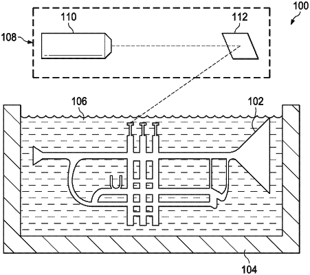
immersing a substrate including at semiconductor die attached thereon in a liquid polymer material:
irradiating part of the liquid polymer material to polymerize and to form a three- dimensional polymer structure on the substrate;
coating the three-dimensional polymer structure with a metal to form a device;
electrically connecting the device with the semiconductor die; and
forming an integrated circuit by encapsulating the semiconductor die and the three- dimensional polymer structure in a package.
|